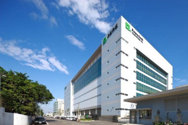
Memory factory Nanya Science and IC design factory Yancai jointly announced today that it has jointly established an AI memory design service company. Nanya Science and Technology and IC Creation will jointly invest NT$500 million in the joint ventu...
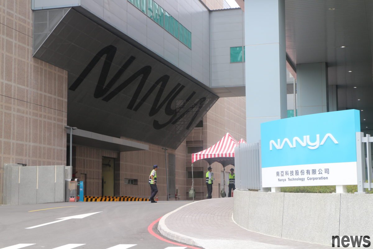
Memory factory Nanya Science and IC design factory Yancai jointly announced today that it has jointly established an AI memory design service company. Nanya Science and Technology and IC Creation will jointly invest NT$500 million in the joint venture with a shareholding ratio of 80:20, respectively, and the company's headquarters is located in Hsinchu City.
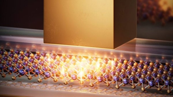
The news draft pointed out that in response to the rapid development of the new AI-side computing market, the two companies will combine dual resources and professional technology, and use Nanyake's advanced process and production capabilities to provide high-added value, high efficiency, and low power consumption customized ultra-high frequency wide memory (HBM) solutions to expand the diversified application vendors of AI-side computing.
Nanyake has always planned to develop HBM. At the beginning of the year, General Manager Li Peiying said that the primary goal of HBM's development is not to enter the data center AI servers HBM3 and HBM3E, which are the least-capitalized data centers, or to return to the HBM2 market, but to target customized products. The reason is that after AI is delegated from the cloud to the end product, it requires more customized high-frequency wide memory. Therefore, Nanya Science and Technology plans to launch new HBM products with its partners at the end of 2026, which will be used for AI PCs, mobile phones, robots, automobiles and other end applications.
Li Peiying also mentioned at that time that HBM R&D requires four major capabilities: high-density design, 3D IC multi-chip packaging, high-frequency wide design, and advanced logical chip-based bare crystal (Base die). Nanyakoin has not invested in the logical process and is working with strategic partners.
Nanyake announced in December 2024 that it will invest its subsidiary Buding Technology with no more than 660 million yuan to combine its customized DRAM product design capabilities to jointly develop high-value and high-efficiency customized high-frequency wide memory solutions. Moreover, Nanyako has also built 3D silicon perforation process (TSV) and multi-chip stacking packaging with its packaging partner Formosako. It can be seen that Nanyako has been working hard on the HBM market and is planning forward with duck paddling.