The new SK Hynix DDR5 memory chip recently appeared on the Internet. It is said to be code-named "X021" and carries a new "AKBD" part code. According to foreign media WCCFtech, the chip first appeared in the Facebook public commu...

The new SK Hynix DDR5 memory chip recently appeared on the Internet. It is said to be code-named "X021" and carries a new "AKBD" part code. According to foreign media WCCFtech, the chip first appeared in the Facebook public community, which seems to mean that it is coming soon.
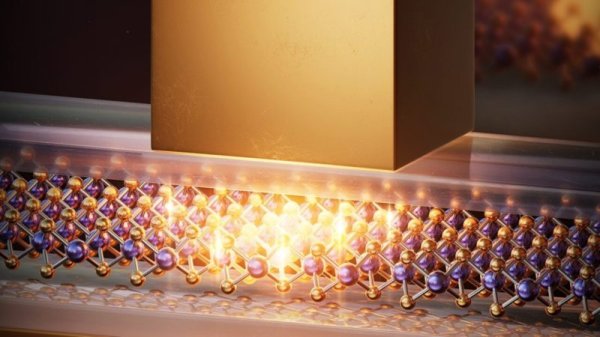
The community post was shared by Kevin Wu of Team Group Technology, and the DDR5 chip is also printed with marks such as "X021" and "AKBD". According to hardware leaker @unikoshardware, the "X021" designation means the second-generation 3Gb A-Die chip, which will replace the 3Gb M-Die currently used in early DDR5 modules.
Currently, SK Hynix has not officially announced this second-generation 3Gb DDR5 A-Die, but according to the naming convention, in the past, codes such as EB, GB, and HB corresponded to the JEDEC standard frequencies of 4,800, 5,600, and 6,400MT/s respectively. Therefore, the new codename "KB" may continue this rule and correspond to the native speed of 7,200MT/s.
In the Facebook community exchange, Kevin also responded that this one is 7,200MT/s, not 5,600 or 6,400.
This new generation of memory specifications also echoes Intel’s future platform roadmap. According to plans, Arrow Lake Refresh and Panther Lake processors are expected to support native DDR5-7200, which is a step up from Raptor Lake's DDR5-5600 and Arrow Lake's DDR5-6400. This means that the new A-Die chip will become the basis for the next generation of high-frequency DDR5 memory modules, specially designed for the new generation of Intel processors.
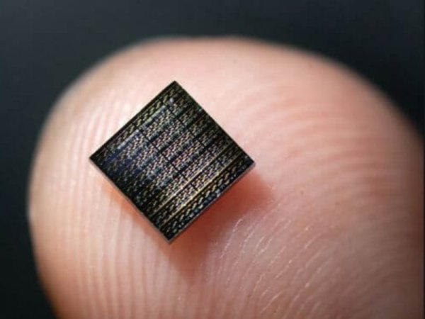
However, some users pointed out that the module shown in the photo may affect high-frequency stability, but it should be considered an early sample of SK Hynix. According to reports, in order to fully realize the potential of the latest A-Die "AKBD" chip, memory module manufacturers must adopt a 10-layer or 12-layer PCB design to truly realize its high-frequency performance.
SK Hynix Second-Gen 3Gb DDR5 “A-Die” Chips Spotted; New AKBD Bin Suggests Native 7200 MT/s Speed Further reading: The deal of the century breaks! OpenAI once considered Google TPU, and Huang Renxun personally took action to win Altman’s heart Arm joins the OCP board of directors and jointly promotes the development of AI data center standards with AMD and NVIDIA