Samsung seems to be postponing the 1.4-nanometer crystalline foundry project originally launched in 2026, and will fully shift the resource focus to the current rapid 2-nanometer process. This shows that Samsung is significantly adjusting its high-l...
Samsung seems to be postponing the 1.4-nanometer crystalline foundry project originally launched in 2026, and will fully shift the resource focus to the current rapid 2-nanometer process. This shows that Samsung is significantly adjusting its high-level process strategy, aiming to re-establish its market position in advanced chip manufacturing under strong rivals such as Tel and Intel.
According to the Korean media "Sedaily", it was reported that Samsung originally planned to build a 1.4-nanometer production line in the second factory area of Pyeongtaek, which was first produced in the second half of 2026. But the project has been postponed, and the latest estimate is 2028, showing that Samsung's development attitude towards the 1.4 nanometers is conservative.
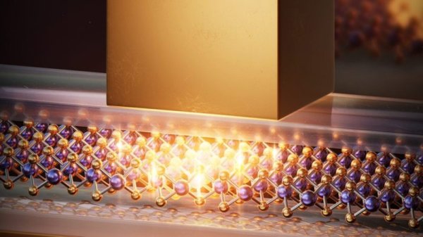
Instead, Samsung is actively promoting the 2nm process and adopting GAA, which means that the yield of this point has increased significantly. It is expected to start production as soon as the end of this year, and plans to lead the 2nm process in the Taylor factory in Texas, USA in the first quarter of 2026, in order to complete the advanced process before TAYO's US factory.
However, the biggest doubts about Samsung are still whether the yield problem has been overcome. Earlier, the yield of Samsung's 2 nanometer process was only about 30%. Although it has increased recently to about 50%, it has not yet been officially certified by the industry and the first batch of manufacturers has not yet been confirmed.
Compared with this, the 2-nanometer process progress of TECHNOLOG is more stable. Foreign-transfer Taiwan power has reached a yield target of 90%, and is expected to officially enter the volume production stage in the second half of this year, and has been adopted by major customers such as Apple, Qualcomm, and Joint Development Corporation. At the same time, the production lines of Taiwan Electric's US factories have also stabilized to supply chips and have begun to have orders.
As for Intel's advanced process, its 18A process currently yields about 50%, and is still being adjusted.
Overall, Samsung is still facing severe challenges in high-level process technology. Although the company has clearly adjusted its direction and hopes to turn around the 2nm process, if there is no clear breakthrough in yield, production capacity, customer layout, etc., it is likely to face a considerable difficulty and pressure if it wants to once again occupy a place in the global semiconductor market in the future.
Samsung Expected to Beat TSMC By Becoming the First Foundry to Introduction Cutting-Edge 2nm Process in the US, With Mass Production at Taylor Facility by Q1 2026 Samsung Is Reportedly Struggling With High-End Nodes as 1.4nm Gets Delayed to 2028, Focus Now Shifted Towards the 2nm Process Extended reading: Taiwan Electric Power Co., Ltd. Google Tensor G5 OEM is difficult to accept, and the strategic meeting review is missing